| |
 |
 |
home |
> |
м ңн’ҲмҶҢк°ң |
> |
кҙ‘н•ҷнҳ„лҜёкІҪ |
> |
LASER CONFOCAL нҳ„лҜёкІҪ |
> |
OLS4500 |
|
|
| |
| LASER CONFOCAL нҳ„лҜёкІҪ |
| OLS4500 |
| New Solutions Made Possible by the OLS4500 |
| |
| Never loses the target once it has been captured. |
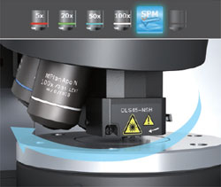 |
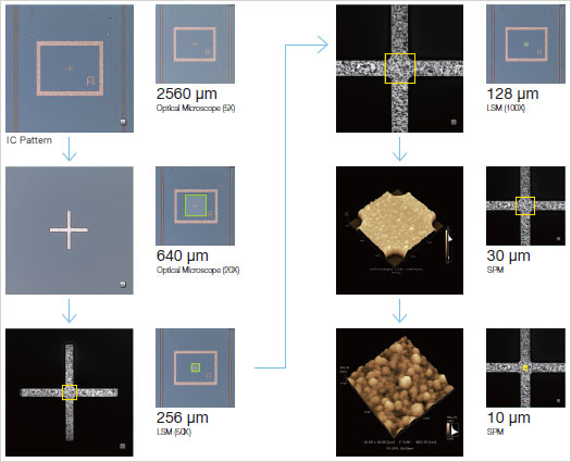
Four objectives ranging from low to high magnifications are installed on the motorized revolving nosepiece together with an SPM unit. The magnification and observation method can be switched seamlessly so that the observation target will remain captured within a field of view. The OLS4500 performs fast search in nano-surface texture. |
| Magnification/Observation Method Switching with Revolving Nosepiece |
| |
|
| A wide range of magnifications and various observation methods enable to detect observation target easily. |
| With a wide range of magnifications and various observation methods, backed by advanced optical technology, the optical microscope makes it easy to locate the observation target. In addition, laser DIC (Differential Interference Contrast) observation enables to visualize nanometric order irregularity in live image. |
 |
 |
 |
| Brightfield Observation (IC Pattern) |
DIC Observation |
Laser DIC Observation |
|
| |
|
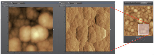
| Reduces the work time from sample placement to image acquisition. |
| Once the sample has been placed on the OLS4500 microscope, all subsequent operations can be performed on the same microscope. The ability to locate the observation target quickly and accurately with SPM allows target image acquisition in one scanning area. |
 |
| |
|
| Integrated design makes it possible to use a single microscope simply by switching the magnification and observation method, without having to remove and replace the sample on another microscope. |
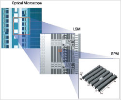 |
As the OLS4500 is an integrated optical, laser and probe microscope system, you can switch between the three microscopic modes as required for observation and evaluation, without having to replace the sample itself. Each of the integrate microscopes is equipped with an array of powerful functions to assure optimum output. |
| |
|
| Seamless Observation and Measurements Made Possible by the OLS4500 |
| |
гҖҗFindгҖ‘Find the Area of Interest Immediately
The OLS4500 Can Quickly Locate the Area of Interest Using a Wid e Variety of Observation Seamless-Magnification Observation Keeping the Object within a Field of View
Methods. |
| A white LED is used as the light source to ensure clear color images with excellent color reproduction. The four objectives enable observation at various magnifications, ranging from low to high. Making full use of the features of optical microscope, the OLS4500 is capable of BF (Brightfield) observation вҖ“ the most commonly used, DIC (Differential Interference Contrast) observation for stereoscopic visualization of fine surface texture by enhancing contrast, and simplified polarized light observation that represents the polarization characteristics of the sample with different colors. Other functions include HDR (High Dynamic Range), which synthesizes several images captured by varying the exposure time to obtain an image with well-balanced brightness and enhanced texture. The OLS4500 can quickly find the area of interest using various observation methods. |
 |
 |
BF Brightfield
Most widely used observation method.
Natural-looking image with realistic color
reproduction. Suitable for observing samples with high contrast. |
DIC
Differential Interference Contrast
Enhances contrast to enable stereoscopic
visualization of samples that cannot be observed with BF. Suitable for detecting defects and foreign matter on samples with mirror surfaces such as metallic structure, hard disks and polished wafer surfaces. |
| |
|
 |
 |
Simplified Polarized Light
Visualization of the polarization properties (e.g. refractive index) of samples by reflected polarized light (light with a specific vibration direction). Suitable for observing metallic surface, minerals and semiconductor materials. |
HDRгҖҖHigh Dynamic Range
Balanced observation of bright and dark regions by synthesizing several images captured by
different exposure time. Fine observation is also
possible by enhancing the texture (surface conditions). |
| |
|
| LSM Can Visualize What Cannot Be Observed with an Optical Micro scope. |
| Thanks to a short-wavelength 405nm laser light, a higher-aperture (high-N.A.) objective lenses and confocal optics, high X-Y resolution is available so that objects not visible with the optical microscope can be observed in clear images. Laser DIC observation makes possible live observation of nanometer micro surface. |
 |
 |
Brightfield Observation
(Foreign Materials on Glass Plate) |
Laser DIC Observation |
| |
|
гҖҗApproachгҖ‘Approach the Area of Interest Quickly and Accurately with SPM
Seamless-Magnification Observation Keeping the Object within a Field of View |
| Four objectives ranging from low to high magnifications are installed on the motorized revolving nosepiece together with the SPM unit. 50X and 100X live observation mode using the optical microscope or LSM places the SPM scanning area in the center of the field. The area of interest can be approached accurately by setting a target mark over the area and switching to the probe scan mode. This means that the target image can be obtained with a single SPM scan, improving work efficiency and reducing wear of the cantilever. |
 |
| |
|
| Guidance for Easy Switching to SPM Observation |
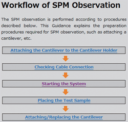 |
Preparations for SPM observation, such as cantilever installation and scanning area setting, can be performed by following the guidance display, which means that even operators with little experience can safely perform preliminary work. |
| |
|
гҖҗNanometric Approach MeasurementгҖ‘Quick Measurement with Simple Operations
Newly Developed SPM Head with Reduced Noise |
 |
The OLS4500 employs a nosepiece-mounting-type SPM scanner head. Because the objective and the cantilever tip are in the coaxial, parfocal positioning, the observation point will not be lost from the field of view even after switching to SPM mode. The newly developed compact SPM head is improved rigidity, so it features reducing image noise and improving responsiveness. |
| Newly Developed Compact SPM Scanner Head |
| |
|
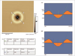
| Navigator to Magnify the Region as Requested |
| The navigator function allows closer viewing of the required region in an image acquired with the probe scan mode by further increasing the magnification. The target image can be obtained by simply setting the magnifying region using the cursor and starting probe scan. The scanning area can be set freely, allowing observation and measurement to be performed more quickly and efficiently. |
 |
| Navigator magnifies a 3.5 Ојm x 3.5 Ојm area on a 10 Ојm x 10 Ојm image |
| |
|
| Analyses to Meet Different Requirements |
 |
Images acquired in SPM measurement mode can be analyzed to suit the requirements of different applications, and the results can be exported as the CSV format. The OLS4500 provides the following analysis functions.
вҖўProfile (curvature factor measurement, contained angle measurement)
вҖўRoughness
вҖўTopography (area, surface , volume, height, histogram, bearing ratio)
вҖўStep ( line, area)
вҖўParticle analysis (optional)
|
| Curvature Measurement (Hard Disk Pits) |
| |
|
| Six SPM Measurement Modes with Easy-to-Follow Guidance Display |
| |
| Contact mode |
| This mode scans the setting area by the cantilever statically while keeping the repulsive force constantly between the cantilever and sample in order to visualize the height information of the sample. It can also be used for the force curve measurement. |
 |
 |
| |
Metallic Thin Film |
| |
|
| Dynamic mode |
| This mode vibrates the cantilever at near the resonance frequency and controls the Z-direction distance to make the vibration amplitude constant in order to visualize the height information of the sample. It is suitable for samples with soft surfaces such as polymers or viscous materials. |
 |
 |
| |
Aluminium Surface |
| |
|
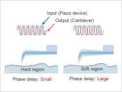
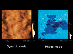
| Phase mode |
| This mode detects phase delays in the cantilever vibration during scanning in the dynamic mode. It can visualize the difference in physical properties on the sample surface. |
 |
 |
| |
Polymer Film |
| |
|
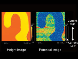
| Current mode |
| This mode applies a bias voltage to the sample to detect and visualize the current flowing between the cantilever and sample. It can also be used for I/V measurements. |
 |
 |
| |
Sample of SiO2 pattern on a Si substrate. The yellow region in the height image (left) is SiO2, which is displayed blue (region without current flow) in the current image(right). These images show that a substrate has regions without current flow. |
| |
|
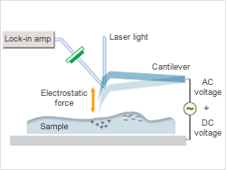
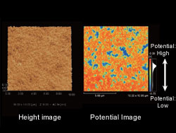
| Surface Potential mode (KFM) |
| This mode applies an AC voltage through the conductive cantilever, detects the electrostatic force working between the cantilever and sample, and visualizes the electric potential on the sample surface. It is also called the Kelvin Force Microscope (KFM) mode. |
 |
 |
| |
Sample of magnetic tape. The surface potential image shows that potential difference of a few hundreds of mV is distributed on the sample surface. This distribution is regarded to reflect the presence of irregularities in the lubrication layer on the tape surface. |
| |
|
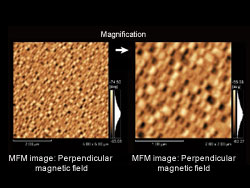
| Magnetic Force mode (MFM) |
| This mode scans the setting area with magnetized cantilever in phase mode and detects the phase delays in the cantilever vibration then visualizes the magnetic information on the sample surface. It is also called the Magnetic Force Microscope (MFM) mode. |
 |
 |
| |
Sample of hard disk. The image shows the distribution of magnetic property. |
| |
|
| LSM allows flexible handling of various samples |
| |
| Imaging Slopes up to 85В° |
| Thanks to dedicated objective lenses with high numerical apertures and a dedicated optical system that obtains superior performance from a 405 nm laser, the OLS4500 can reliably measure acute-angled samples that were previously impossible to measure. |
 |
 |
| LEXT-Dedicated Objective Lenses |
Razor with an Acute Angle |
| |
|
| Micro-Profile Measurements with High Resolution |
| Thanks to a short-wave length 405 nm laser light and a higher-aperture objective lens, 0.12 Ојm X-Y resolution is available. As a result, the OLS4500 can perform submicron measurements of sample's surface. Combined with a high-precision linear scale and Olympus original intensity detection technology, this allows high-definition imaging, enabling accurate height measurement from the submicron to the hundreds of microns range. In addition, the OLS4500 is able to assure both "accuracy", which indicates how close a measurement value is to its true value and "repeatability", which indicates the degree of variations among repeated measurement values, both show the performance of measuring tool. |
 |
 |
| 0.12 Ојm Line and Space Pattern |
(MPLAPON50XLEXT)
STEP Height standard Type B, PTB-5, Institut fГјr Mikroelektronik, Germany, 6 nm Detection in Height Measurement |
| |
|
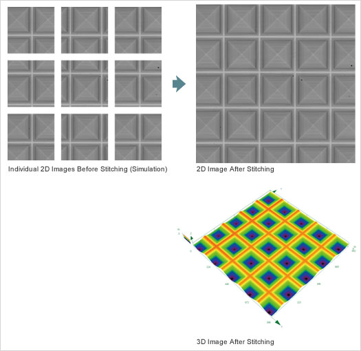
| Designation of Any Image Capturing Area from a Wide Area |
| Though the field of view at high-magnification image is narrow in general, the stitching function of the OLS4500 can provide image data with high resolution and a wide field area by stitching together up to 625 images. The obtained wide-field image can be subjected to 3D display and 3D measurement. |
 |
| |
|
| Non-Contact Measurement of Surface Roughness of Micro Area |
| |
| Enables Plane Roughness Measurement in Addition to Line Roughness |
| Thanks to dedicated objective lenses with high numerical apertures and a dedicated optical system that obtains superior performance from a 405 nm laser, the OLS4500 can reliably measure acute-angled samples that were previously impossible to measure. |
 |
With continuous reductions in the size and weight of recent industrial products, the parts composing them are also subject to miniaturization. This trend toward micro-miniaturization of component parts is increasing the importance of surface roughness measurement, as well as geometry measurement. Reflecting these market needs, the ISO added the LSM and AFM to the list of 3D surface texture measuring instruments (ISO 25178-6). This means that non-contact surface roughness measurement is recognized as an official evaluation standard just like the traditional contact surface roughness gauge . The OLS4500 comes with roughness parameters conforming to the ISO. |
| |
|
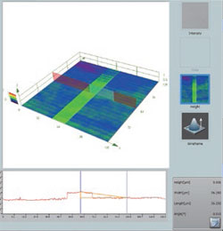
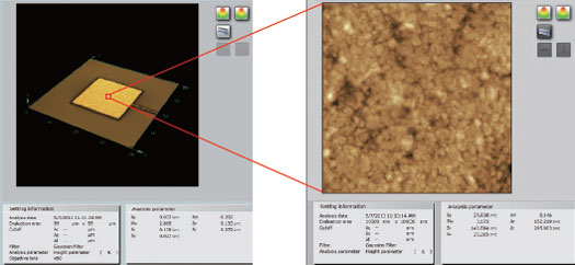
| Plane Roughness Measurement for Capturing Detailed Information |
| Non-contact surface roughness measurement can obtain the plane roughness as well as the line roughness. The plane roughness measurement can also identify roughness distribution and properties in a region designated on the sample surface so that they can be collated with the 3D image for evaluation. The OLS4500 can measure the surface roughness using either the LSM or SPM function. These two functions can be selected according to the sample properties or observation purpose. |
 |
Plane Roughness Measurement with LSM
(105 Ојm x 105 Ојm) Bonding Pad |
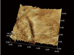
Plane Roughness Measurement with SPM
(10 Ојm x 10 Ојm) |
| |
|
LEXT OLS4500 Parameters
Parameter Compatibility |
| The OLS4500 comes with the same Surface Profile Parameters as contacttype surface roughness gauges, offering compatible operability and measurement results. |
| |
|
| Primary Profile |
Pp, Pv, Pz, Pc, Pt, Pa, Pq, Psk, Pku, Psm, PО”q, Pmr(c), PОҙc, Pmr |
| Roughness Profile |
Rp, Rv, Rz, Rc, Rt, Ra, Rq, Rsk, Rku, Rsm, RО”q, Rmr(c),RОҙc, Rmr, RZJIS, Ra75 |
| Waviness Profile |
Wp, Wv, Wz, Wc, Wt, Wa, Wq, Wsk, Wku, Wsm, WО”q, Wmr(c), WОҙc, Wmr |
| Bearing Area Curve |
Rk, Rpk, Rvk, Mr1, Mr2 |
| Motif |
R, Rx, AR, W, Wx, AW, Wte |
| Roughness Profile (JIS 1994) |
Ra(JIS1994), Ry, Rz(JIS1994), Sm, S, tp |
| Others |
R3z, P3z, PeakCount |
|
| |
|
| Accommodating Next-Generation Parameters |
| The OLS4500 comes with roughness (3D) parameters conforming to ISO 25178. By evaluating the planer area, high-reliability analysis is made possible. |
| Amplitude Parameters |
Sq, Ssk, Sku, Sp, Sv, Sz, Sa |
| Functional Parameters |
Smr(c), Sdc(mr), Sk, Spk, Svk, SMr1, SMr2, Sxp |
| Volumetric Parameters |
Vv(p), Vvv, Vvc, Vm(p), Vmp, Vmc |
| Lateral Parameters |
Sal, Str |
|
| |
|
| Microscope Technologies of the OLS4500 |
| |
| Principles and Features of Optical Microscope |
 |
The optical microscopic image using visible light range (400 to 800 nm wavelength) enables observation at magnifications ranging as high as approx. 1000x. The optical microscope makes it possible to observe a sample in color, to enhance surface texture by switching the observation method, and to observe substances by taking advantage of their properties (polarization property). The OLS4500 can apply the following observation methods.
вҖўBrightfield observation
Most popular observation method. Forms an image from the light reflected from the sample surface.
вҖўDifferential Interference Contrast (DIC) observation
3D visualization of fine surface irregularities on the sample by enhancing the contrast.
вҖўSimplified polarized light observation
Visualizes the polarization property of the sample using incident polarized light (light with a specific vibration direction)
|
| Brightfield observation can provide color information. Ink-jet dots. |
| |
|
Principles and Features of Laser Scanning Microscope
LSM (Laser Scanning Microscope) Facilitates Submicron Observation and Measurement |
 |
The X-Y plane resolution of an optical microscope depends greatly on the wavelength of the light used. The LSM employs short-wavelength light so its X-Y plane resolution is superior to that of a traditional microscope which uses visible light. The OLS4500 incorporates a laser light with a short wavelength of 405 nm and combines a dedicated high-aperture (high-N.A.) objective and confocal optics to achieve X-Y plane resolution of 0.12 Ојm. Its XY scanning function - which uses an Olympus-original 2D scanner - makes possible high-resolution scanning of 4096 x 4096 pixels (max.). |
| High-Resolution XY Scanning of Laser Microscope (image illustration) |
| |
|
| Superior Height Measuring Capability |
 |
The LSM employs a short-wavelength semiconductor laser light and confocal optical system to detect in-focus images, while eliminating out-offocus images. Combined with a high-precision liner scale, this allows highdefinition imaging, enabling accurate 3D measurement. |
| Step Difference Measurement |
| |
|
Principles and Features of Scanning Probe Microscope
SPM (Scanning Probe Microscope) Visualizes the Nanometric-Order World |
 |
SPM is the generic name of microscopes which perform 3D type observation of samples by approaching a small probe with a tip curvature of about 10 nm to the sample surface and scanning the sample, while detecting the dynamic and electrical interactions between the probe and sample. One of the typical SPMs is the AFM (Atomic Force Microscope), which images minute surface texture of the sample by detecting the attractive and repulsive forces between the probe and sample surface. Observation at the nanometric level makes it possible to capture the texture of the sample finely. |
| Principles of Probe Microscope |
| |
|
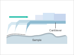
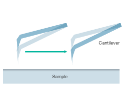
| Nanometric Observation by Cantilever Scanning |
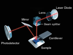 |
The OLS4500 employs an optical lever system that can detect the micro-deflection (displacement) of the cantilever carrying the probe on the tip with high sensitivity. By reflecting the laser beam on the back of the cantilever and applying Z-axis drive using a piezo device, the beam hits the specified point on the photodetector so that the system can read a minute Z-direction displacement. |
| Optical Path of SPM Sensor |
| |
|
| Various Modes for Imaging Surface Texture Figure and Physical P roperties |
 |
Polymer Film The scanning probe mode incorporates various modes for use in texture observation and measurements of the sample surface, as well as for analysis of the physical properties. The modes available with the OLS4500 are as follows.
вҖўContact modeпјҡ Surface texture visualization (hard surface)
вҖўDynamic modeпјҡ Surface texture visualization (soft surface, viscous surface)
вҖўPhase modeпјҡ Visualization of physical differences on the sample surface.
вҖўCurrent mode*пјҡ Detection and visualization of current flowing between the probe and sample.
вҖўSurface potential mode (KFM)*пјҡ Visualization of electric potential on the sample surface
.
вҖўMagnetic force mode (MFM)*пјҡ Visualization of magnetic information on the sample surface.
* Optional.
|
| Polymer Film |
| |
|
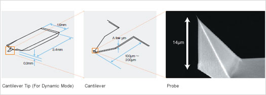
| Cantilever: Key to the High Definition and Quality of an Image |
| The probe is placed on the tip of a sheet-type cantilever with a length of approximately 100 to 200 Ојm. The spring constant and resonance frequency of the cantilever are selected according to the sample feature. As the probe wears after repeated scanning, the cantilever tip should be replaced either periodically or as required. |
 |
| |
|
|
|
|
|
|
|
| |
|