| |
 |
 |
home |
> |
м ңн’ҲмҶҢк°ң |
> |
м „мһҗнҳ„лҜёкІҪ |
> |
нҲ¬кіјм „мһҗнҳ„лҜёкІҪ(SEM) |
> |
JEM-ARM200F |
|
|
| |
| нҲ¬кіјм „мһҗнҳ„лҜёкІҪ(SEM) - JEOL |
| JEM-ARM200F |
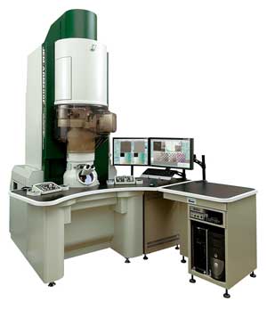
| JEM-ARM200F Transmission Electron Microscope |
The JEM-ARM200F, incorporating a spherical aberration corrector for electron optic system as standard, has achieved a scanning transmission image (STEM-HAADF) resolution of 0.08 nm, the highest in the world among the commercial transmission electron microscopes.
|
 |
- World's highest STEM (HAADF) resolution of 0.08 nm guaranteed
The ARM200F, incorporating a spherical aberration corrector for electron optic system as standard and the maximum level of electrical and mechanical stability, has achieved a scanning transmission image (STEM-HAADF) resolution of 0.08 nm, the highest in the world among the commercial transmission electron microscopes.The electron probe, after its aberrations are corrected, features a current density level higher by an order of magnitude than conventional transmission electron microscopes.With this probe finely focused, the ARM200F is capable of atomic level analysis, substantially reducing measurement time and imoproving throughput.
- Enhanced electrical stability
To achieve an atomic level resolution, the power supply to control the electron optic system needs to be stabilized.The ARM 200F has reduced the fluctuation of high voltage and objective current by 50% of conventional transmission electron microscopes, significantly enhancing its electrical stability.
- Enhanced mechanical stability
To enable atomic level analysis and imaging utilizing spherical aberration correctors for electron optic and image forming systems, vibration and distortion on the atomic level need to be controlled.The ARM 200F features an overall mechanical strength twice higher than conventional transmission microscopes by enlarging the coolumn size to improve the rigidity and optimizing the console structure, enhancing mechanical stability.
- Wide ranging STEM analytical capabilities
Two types of dark area detectors with different STEM detection angles (one as standard), bright area detector (standard), and backscattered electron detector (option) can be simultaneously installed.A new scanning image acquisigion system is capable of acquiring 4 different types of signals, enabling simultaneous observation of these 4 images.
- Environmental measures
Atomic level vibration and distortion are also caused by changes in temperature and stray magnetic field in the instrument room.The ARM 200F features a set of thermal and magnetic shields as standard.The column is also housed in a cover to prevent the column surface temperature from fluctuating as the ambient convection changes.
- Optional spherical aberration corrector for image forming system
With an optional spherical aberration corrector, the resolution of transmission electron microscope image (TEM) can be improved to 0.11 nm.
|
|
|
|
| |
| JEM-ARM200F Specifications |
| Resolution |
| Scanning transmission image?1) |
0.08 nm 2)?(at 200kV) |
Transmission image
Point image
Lattice image |
0.19 nm (at 200kV)
0.11 nm with TEM Cs corrector 3) (at 200kV)
0.10 nm |
| Magnification |
| Scanning transmission image |
200 to 150,000,000x |
| Transmission image |
50 to 2,000,000x |
| Electron gun |
Schottky field emission gun |
| Accelerating voltage |
80 to 200 kV 4) |
| Specimen Stage |
| Stage |
Eucentric side entry goniometer stage |
| Specimen size |
3 mm dia. |
| Tilt angle |
Up to 25В° (with double tilt holder) |
| Movement range |
X/Y: Вұ1.0 mm (motor drive/piezo drive) |
| Cs Correctors |
| STEM Cs corrector |
Standard |
| TEM Cs corrector |
Optional |
| Optional accessories |
Energy Dispersive X-Ray Spectrometer (EDS)
Electron energy-loss spectrometer (EELS)
CCD camera, etc. |
|
| |